The Optical Race of 2026: Google, NVIDIA and the Three Waves of Photonics
Google runs optical switches in production, Ayar Labs raises $500M, Celestial AI joins Marvell. Three waves of photonics and the consequences for AI.
Key takeaways
- The wall AI is hitting is not logic but data movement: energy goes into moving bits, not arithmetic. The physics of this is in the first part of the diptych.
- Google remains the only company to publicly describe such a large-scale production deployment of optics: the Apollo project forms the basis of most of its data-center networks.
- Scale on optics: Google connects up to 9,216 Ironwood TPUs into a single supercomputer versus a maximum of 72 GPUs over NVLink — a 128x gap delivered by the optical interconnect, not the chip.
- The wave of 2026 is co-packaged optics: Ayar Labs ($500M Series E; strategic investors AMD, NVIDIA, MediaTek), Lightmatter (record 1.6 Tbps per fiber), Celestial AI / Marvell (compute–memory disaggregation).
- The optics market for AI clusters grew from $16.5B (2025) to $26B (2026) — up 60% in a year. The third wave — photonic accelerators and memory (Lightelligence, Q.ANT, Lumai) — is still frontier.
- Optics removes the bottlenecks of movement and multiplication, but does not remove the questions of the loop: light reads the archive faster, but the archive remains an archive. Whoever owns the optical domain gets an order of computation.
A signal that cannot be ignored
In March 2026 something happened on the semiconductor market that occurs once every few years: strategic investors — including direct rivals AMD and NVIDIA, plus MediaTek — simultaneously entered the optical startup Ayar Labs, which had raised $500 million. When sworn competitors bet on one platform, it is a rare signal: they all see a wall they are about to hit together. And that wall is not logic and not transistors.
Most of the energy of a modern AI processor goes not into arithmetic but into moving data — between the compute unit and memory, between chips, between racks. This movement is the most expensive and fastest-growing cost item. The physics of why light moves data cheaper than the electron is covered in the first part of the diptych. Here: who is breaking this wall in 2026, how, how much money it takes, and what it changes for the industry.
How the industry got here
Ten years ago photonics seemed a niche technology for telecommunications. Then the growth of AI cluster sizes turned interconnects into the main energy limit. That is when developments that had long stayed in the lab began moving into the infrastructure of the largest data centers. By 2026 this transition had stopped being an experiment and became a race.
The bottleneck is movement, not computation
Engineers call this two walls. The memory wall — the gap between the speed of the compute unit and the speed at which it gets data from memory. The interconnect wall — the cost and latency of moving data between chips. Both walls are about the same thing: about movement.
From this follows a non-obvious but precise observation: the waves of photonics arrive exactly in the order in which the industry hits bottlenecks. First light takes over movement — the most expensive operations, interconnects and switching. Then multiplication, the most frequent operation of neural networks, which is convenient to perform by interference. And only at the end — storage, the hardest one, because a photon cannot be stopped. This order is not a roadmap coincidence. It repeats the order of the walls.
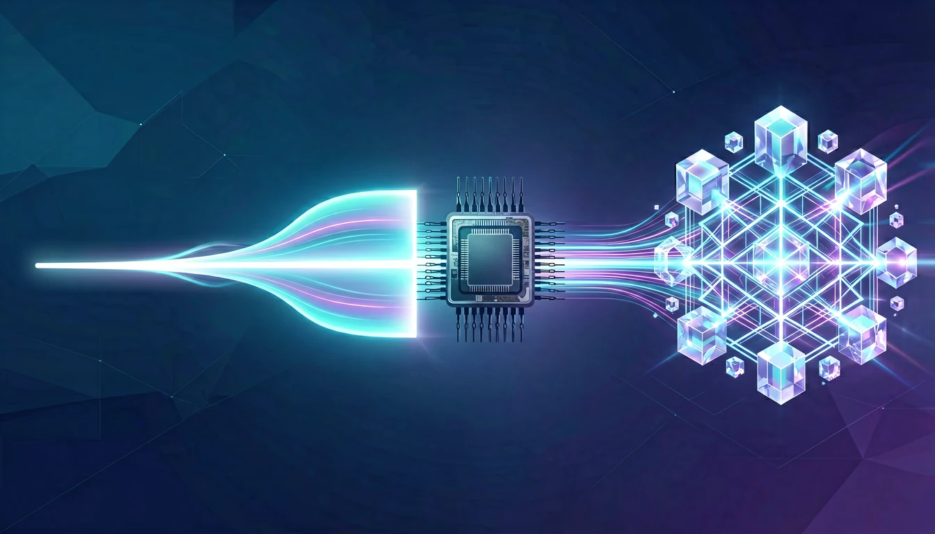
Wave 1. Google: optics already in production
The company that so far is the only one to publicly describe such a large-scale production deployment of optics is Google. Its Apollo project is one of the first publicly described large-scale production deployments of optical circuit switching (OCS) in data-center networks, reflected in the works of Urata and co-authors (2022–2023). Optical switches replaced traditional packet switches in the Jupiter architecture and, in Google's own words, "form the basis of the vast majority of our data-center networks". According to an independent estimate by SemiAnalysis, Apollo's effect on Google's data-center networks exceeds $3 billion — a figure the company has neither denied nor directly confirmed.
What this gives in practice is visible in the accelerators. Google's TPU Pods are connected through optical switching: light is switched at the level of physical circuits, without electro-optical conversions at every hop. The result is scale unattainable for electronic interconnects: Google assembles up to 9,216 TPUs of the Ironwood generation into a single supercomputer, while NVIDIA's NVLink confines a domain to 72 GPUs. The 128x gap is not a difference in chips. It is a difference in interconnect physics.
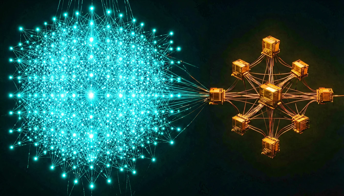
It is important not to mix up generations and their statuses. Ironwood (TPU v7) is already in general availability and runs in production: Google calls it "the first TPU for the inference era" — a tenfold increase in peak performance over v5p and 9.6 Tbps of aggregate bidirectional bandwidth per chip over four ICI links. Those 9,216 chips are Ironwood reality.
The eighth generation — TPU 8t and 8i, "two chips for the agentic era" — was announced in 2026, but it is a preview with shipments stated for 2027: a separate die for training (8t) and a separate one for inference (8i). The stated scale of the 8t pod — up to 9,600 chips and 121 exaflops on FP4 — is an announcement, not production reality, and it should not be mixed with the 9,216 Ironwood TPUs. Cignal AI analysts directly link the growth in demand for optical switches in 2025–2026 to Google's TPU deployment pace.
Google did not wait for photonics to mature. It built production on it.
Wave 2. Light reaches the chip: co-packaged optics
The second wave brings light right up to the die. Optical modules move into the same package as the silicon (co-packaged optics, CPO), removing the copper "last centimeters". The 2026 chronology reads like a race:
- Ayar Labs closed a $500M Series E (March 3, 2026) for volume production of CPO for AI scale-up. Strategic participants — AMD, NVIDIA and MediaTek; the financial lead was Neuberger Berman, with ARK Invest, Insight Partners and the Qatar Investment Authority among the investors. Rivals AMD and NVIDIA on one platform — that very signal from the opening.
- Lightmatter (MIT spin-off) demonstrated a record 1.6 Tbps per fiber and the Passage CPO chiplet at Computex/OFC in March 2026.
- Celestial AI with Photonic Fabric — up to 172.8 Tbps in the second generation of chiplets — joined Marvell: optics became part of a major semiconductor vendor's product line.
The meaning of this wave is disaggregation. If light is cheap per bit and per distance, the compute unit and memory can be spread across different dies and even racks without losing bandwidth. Celestial AI claims a 25x increase in bandwidth at a 10x reduction in energy per bit versus electrical interconnects. This is a direct strike at the memory wall — no longer the interconnect as a cable, but the interconnect as an architecture.
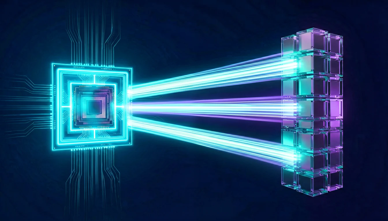
Wave 3. Photonic computing and memory: the frontier
The third wave — light begins not only to move, but to compute. At WAIC 2026 Lightelligence showed PACE 3, a photonic chip with a 256×256 matrix core; for comparison, Google's TPU matrix blocks have stabilized at 256×256 for years, and photonics is reaching the same operation form-factor. German Q.ANT launched the second generation of its photonic processor in June 2026, on which generative and recurrent networks are already running. British Lumai released an optical system for inference of billion-parameter models; a paper on an analog optical computer for AI inference and combinatorial problems was published in Nature (2025).
The hardest layer is photonic memory. And it also produced the most telling recent result: the pLatch by the UW–Madison and USC ISI team, presented at IEEE IEDM 2025 — a fab-manufactured optical cell with write speeds of about 20 GHz and read speeds of 50–60 GHz. The physics of why memory is photonics' weakest link is covered in the first part; here it is enough to say that a mature DRAM analog is years away.
What this changes for the industry
Inference becomes the main battlefield
The economics of AI have shifted from training to inference: reasoning models and agents spend orders of magnitude more compute on generation than on training. It is no coincidence that Google calls Ironwood "the TPU for the inference era", and the eighth generation splits into a training and an inference die. Photonic accelerators strike exactly here: matrix operations in light, with an energy-per-operation advantage, make long reasoning and multi-step agent loops economically viable.
Cluster scale as the new currency
Frontier models are trained and served by clusters, and the cluster ceiling is set by the interconnect. Optics allows assembling tens of thousands of accelerators into a single computer: 9,216 Ironwood TPUs vs 72 GPUs — a demonstration that optical topology scales where electronic domains fall apart. The consequence is a new line of competition: not "whose chip is faster" but "whose optical domain is bigger".
Energy and geography
AI data centers have approached gigawatt-scale power, and energy has become a political and economic limit on growth. Optics lowers energy per bit in transmission and per operation in matrix multiplication, easing the main bottleneck of expansion — the power grid. The race is distributed unevenly across regions:
| Region | Key players | Specialization |
|---|---|---|
| USA | Google (Apollo, TPU), Ayar Labs, Lightmatter, Celestial AI / Marvell, NVIDIA (SiPh in its own architectures) | OCS in production, CPO, photonic accelerators |
| Europe | Q.ANT (Germany), Lumai (UK), Nokia Bell Labs, imec (Belgium), PhotonDelta (Netherlands) | Photonic processors and memory cells, PIC fabs |
| Asia | Lightelligence, NTT (Japan), MediaTek, Korean foundries (SiPh in HBM and logic) | Photonics integration into memory and volume production |
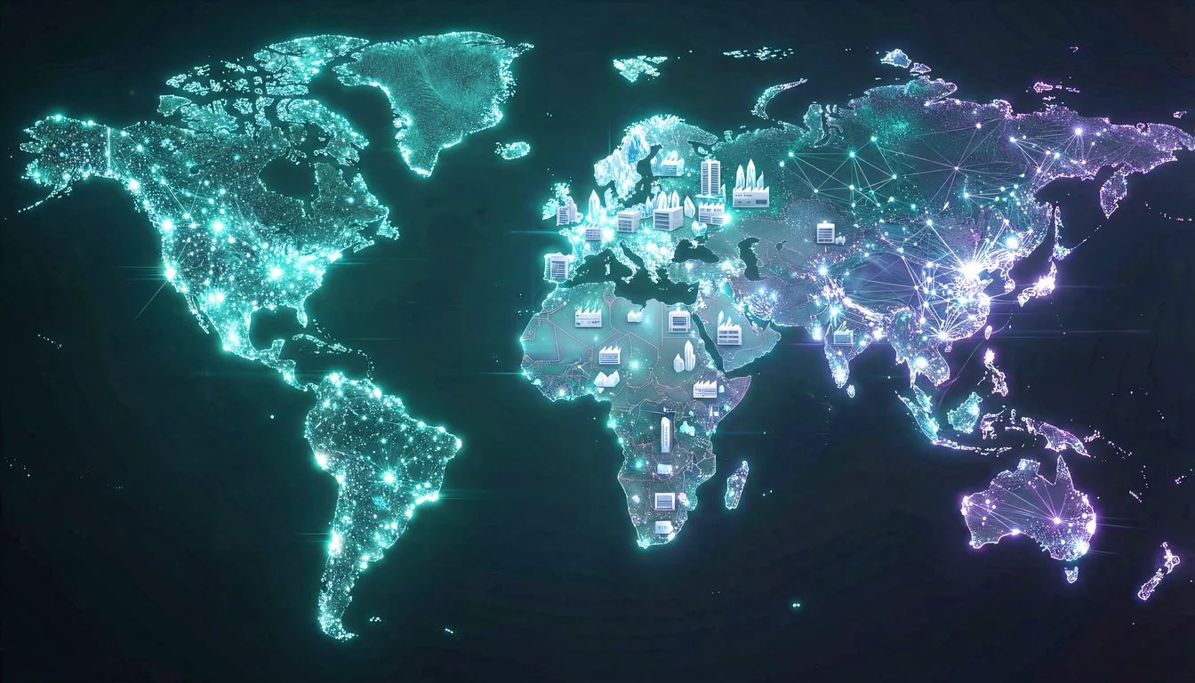
The USA leads at the systems level. Europe at the device level. Asia at the level of integration into mainstream semiconductors.
Risks: why the wave may break
Analog noise. Photonic matrix cores are analog, with an effective precision of about 5–8 bits in current prototypes. That is enough for inference, not for training with gradient accumulation. So optics will remain an inference technology in the coming years.
No memory and no nonlinearity. Light does not store state and does not control itself: logic and memory require conversion back into electronics. A purely optical computer is a physically incorrect goal; the real bet is a hybrid, and success depends on the quality of hybridization, not on the "purity" of optics.
Manufacturing hell. Photonic circuits are more sensitive than CMOS to process variation: nanometer tolerances, die yield, packaging of lasers and detectors. Volume CPO production in 2026 is a stated goal, but stated and mastered are different stages.
The software stack. Photonics has no CUDA of its own: compilers, operation maps, debugging tools are only emerging. The industry remembers that the GPU victory was won not by the transistor but by the software ecosystem. Without a stack, even a perfect die remains a lab artifact.
NVIDIA adapts. The leader does not wait for the wave — it builds it in. In the accelerator architectures presented at IEDM 2024, silicon photonics was placed at the center of chip design, and NVIDIA's investment in Ayar Labs means optics will become part of the NVLink ecosystem, not its killer. The history of GPUs absorbing many specialized accelerators is a direct warning to photonic startups.
Marketing dilution. "100 times faster than GPU" in press releases is usually the speed of a single matrix operation under ideal conditions, not a system end-to-end result. The system metric — cost and energy per useful task — is rarely published for photonics. The same term-dilution trick as in "agentic AI", which we wrote about earlier.
The conceptual frame: the archive and the caste
In our materials on agents and the loop we described a system locked in an archive — in the data and weights it samples from. So here is the thing: the bottleneck of this loop is not computation but movement: the archive grows faster than the medium can carry it. The memory wall and the interconnect wall are the physical walls of the archive: copper cannot keep carrying the past to the compute unit fast enough. Optics first removes the movement bottleneck, then the multiplication bottleneck, and only then — if it works out — the storage bottleneck. The order of the waves repeats the order of the walls.
And here is the limit of optimism that should be stated plainly. Optics accelerates moving and fetching from the archive, but it creates nothing new: the photonic loop remains a loop locked in the same archive, only now it reads it at the speed of light. A change of carrier changes the reading speed, not the nature of the system. The questions of goal-setting, responsibility and diversity raised in the agent materials are not removed by any physics of the carrier.
Light reads the archive faster. But the archive remains an archive.
Finally, the caste layer. Optical supercomputers are an expensive resource, and access to them stratifies the industry even harder. Whoever owns an optical domain of nine thousand accelerators obtains an order of computation unavailable to someone renting GPUs by the hour. The gap between the "augmented" and the "prosthetized" in the agent economy gains physical infrastructure.
Conclusion
Optical computing in 2026 is no longer a promise. Google has been running optical switches in production for years, Ironwood runs in general availability, the eighth-generation TPU is announced for 2027, Ayar Labs and Lightmatter are bringing CPO to volume production, and photonic accelerators are reaching the matrix-operation form-factor familiar from TPUs. The optics market for AI clusters has grown 60% in a year.
But a sober view matters just as much. Optics removes the walls of movement and multiplication without removing the constraints of precision, memory and logic; manufacturing and the software stack are not yet mastered; and NVIDIA is building light into its own ecosystem rather than letting the wave pass by. This is not a "silicon killer" — it is a new physical layer inside the hybrid.
In the history of computing there have already been changes of architectures, languages and algorithms. Today, for the first time in decades, the physical medium of computation itself is changing. Perhaps one day this very transition will be regarded as the beginning of a new era in computer engineering. The only question is who will own this medium — because light reads the archive faster for everyone, but the archive itself, and power over it, does not disappear.